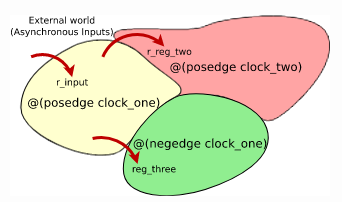
Crossing Clock Domain inside of an FPGA is a common task. Problems can occur if the digital designer does not understand all of the details involved in crossing from one clock domain into another. A single clock domain entails all of the Flip-Flops that are driven by one.
Crossing from slower clock domain to faster clock domain
The simplest type of crossing is going from one clock domain to a faster clock domain. In this type of crossing, you are still subject to Metastability, but the fix described in that article works very well in this situation. All you need to do is "double-flop" the data, which is shown in the figure below.

The slower clock is your source clock domain. The faster clock is your destination clock domain. In the faster clock domain, the first Flip-Flop has a metastable output. The reason this occurs is that performing this crossing, there will be violations of setup and hold time which are the cause of metastability. You can work around this by simply double-flopping the data on in the faster clock domain. The output of the second Flip-Flop will be stable and now the data can be used in the faster clock domain.
The code below shows how you might look for a rising edge on a signal when crossing from a slow to a fast clock domain. Note that your logic for the edge-detection must be done in the fast clock domain.

Crossing from faster clock domain to slower clock domain
This situation is slightly more complicated than the previous one. Here we are going from a fast clock domain to one that is slower. In this situation, it is easy to imagine an example where the data inside the fast clock domain might change before the slow clock domain even sees it.
For example, consider a pulse that occurs for 1 clock cycle in a 100MHz clock domain, that you are trying to sample in a 25MHz clock domain. There is a good chance that you will never see this pulse if you simply sample the data with your 25MHz clock. In order to transfer a signal from a fast clock domain to a slow clock domain you must stretch out your signal. Refer to the figures below for a visual representation of this.


Stretching your data occurs when you stretch out a pulse or data long enough to guarantee that the slow clock domain has a chance to sample it. In the example above, you would need to stretch out your data to ensure that setup and hold times are met no matter when the data is sampled. To properly guarantee that setup and hold times are met, I recommend stretching out your pulses such that they take at least 2 clock cycles in the slow clock domain. So in the example above, you should stretch out the 100MHz pulse to at least 8 clock cycles you can always go more.
Crossing between clock domains with lots of data( FIFO)
I saved the best for last. By far the most common way to send data between two clock domains is to use a FIFO. The one requirement here is that you need to make sure that the FIFO you use supports two different clock frequencies. Some FIFOs only support one clock. When crossing from one clock domain to another, you must ensure that the two cardinal rules of FIFOs are maintained
- Never write to a full FIFO
- Never read from an empty FIFO
As long as those two rules are maintained you will be fine. Since your clock domains are different, you need to keep in mind the level of the words in your FIFO. This is often done best using the Almost Full (AF) and Almost Empty (AE) FIFO flags. So think about your situation and make sure that both the read and the write sides of your FIFO will be okay.
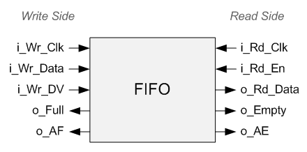
The Almost Full (AF) flag and Almost Empty (AE) flag are your best friends. Many FIFOs offer you a count of the words inside the FIFO, but I do not recommend ever using this. Additionally, if you write your code correctly, you shouldn't need to rely on the Empty or Full flags either, just the AE/AF flags.
Consider a case where we have some module writing data to a FIFO at 33MHz. On the read side, we are dumping the data as quickly as possible to external memory. Let's say the read clock is 110MHz. In this situation, we can see that the read clock is much faster than the write clock, so even if the writes were happening at ever clock cycle, the read side will still be idle much of the time. The way to handle this is to set your Almost Empty flag to some number that indicates to your read code that there is a burst of data ready for the read module.
Let's assume this gets set to 50 words. Once the FIFO has 50 words inside of it, the AE flag will transition from 1 to 0, which will trigger some logic to drain exactly 50 words from the FIFO. This is often how crossing clock domains gets implemented. If you are using your AE/AF flags, you're doing it correctly. Try not to rely on your Empty or Full flags, and definitely do not use the FIFO count that some FIFOs support.
Timing errors and crossing clock domains
Commonly when you cross clock domains you will experience timing erros. This is the tools telling you that you will have asituation where your setup and hold times are not going to hold and that you will have a metastable condition. Metastability is common timing constraints that relax the tools and tell them that you're a competent designer and that you understand that your design can be metastable.
You should always aim to have no timing erros in your design. Exactly how to create these timing constraints is beyond the scope of this article. Refer to your FPGA vendor use guides for details of this.
In summary, as an FPGA designer you will experience situations where you cross clock domains. You need to clearly understand the common pitfalls that occur in these situations. If the crossing is simple enough, you can just double-flop the data or perform pulse stretching. For the majority of situations, you'll likely need to use a FIFO that supports two clocks, one for reading and one for writing. When structuring your cross clock domain code, be very careful not to mix and matach signals from both clock domains.
Reference: zipcpu.com/blog/2017/10/20/cdc.html
'Semiconductor > ASIC & FPGA' 카테고리의 다른 글
| Debounce a Switch in a FPGA (0) | 2020.11.15 |
|---|---|
| Block RAM( BRAM) (0) | 2020.11.12 |
| Timing (0) | 2020.11.09 |
| Propagation Delay (0) | 2020.11.08 |
| Shift Register (0) | 2020.11.08 |


